Relay 4-Bit Ripple Carry Adder

After developing relay based logic gates and designing 1 bit full adder made from relays, the challenge was to link a few of these together to create a relay based binary adder.  The overall objective was to create a relay based adder that could handle calculations of at least a moderately interesting size. A 4 bit adder seemed like a good place to start, since 4 bits is enough to express numbers higher than what I can count on one hand.

Because my full adder design can take 3 inputs (A,B and a carry) and  produces a sum and carry bit, all that needs to be done is to connect them together end-on-end:
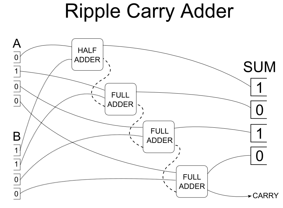
4-bit relay ripple carry adder

I have abstracted my adder designs into little boxes here in this schematic, but each box is just a placeholder for the adder designs I showed in the previous post.

This kind of adder is called a ripple carry adder as each 1 bit calculation ripples down the line rolling into each adder below it.  For my little 4-bit adder this works perfectly speedily, but if you wanted to build something more sophisticated this mode of calculation would be painfully slow, especially with mechanical switches like relays.

You may have astutely noticed that the first adder in the series is only a half adder.  This is because I don’t need to handle a carry bit on the first addition since there isn’t anything before it.

In the example schematic I am adding 2 (Input A) to 3 (Input B).  The sum is of course 5. This is the same inputs I used in my excel adder in the previous post, just so you can see how the addition works.  While the final carry is unused in this example, having a carry on the final bit brings the total output display up to 5 bits, therefore it is possible to add any two numbers with a product of less than 31.  Definitely not an amazing adding machine, but it does help me to understand how applying and not applying current can model binary math in a circuit.

Check out the working relay 4-bit ripple carry adder I breadboarded in this high octane video (I apologize for my video editing skills):

Since designing my 4-bit adder, I have done a little reading and discovered a full-adder circuit that uses 2 relays rather than 6.  If the java applet will load, you can view the example on with this University of Hamburg app.
Relay Full Adder Circuit

Having designed some logic gates using relays, I had the foundations of doing simple math with a pure relay circuit.  This is where the adder comes into play.

To understand how adders work you really have to start with a brief discussion of base 2 vs base 10 mathematics.  Everybody should be familiar with base 10.  It is the common mode of mathematics where there are 10 possible numbers (1,2,3,4,5,6,7,8,9,0) that are used in a particular way to represent all numbers.  However, base 2 is the number system that most computer use.

Understanding BASE 2 (BINARY)

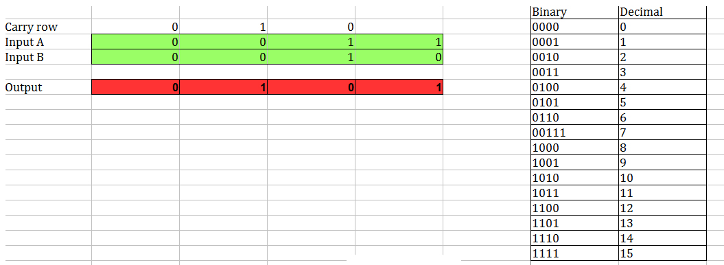
Base 2, also known as binary, uses only 2 numbers (1 & 0).  This makes it possible to represent a full numerical system using the electrical concept of charge (1) or no charge (0).  Meaning that those on or off inputs and outputs into logic gates allow us to build a system that can do calculations.  To better understand this for myself, I setup a 4 binary adder in Excel so that I could really see how this math works.

binary adder excel

Feel free to download the 4-bit Binary Adder if you want to mess around with it.

In this example screenshot I am adding 3 + 2 (look at the key to the right for a conversion to base 10.)  To work with adding binary numbers we start from the right and work our way left, always thinking about SUM and CARRY.  Here is my break-down of the step-by-step addition of 3 + 2 in binary:

Starting on the far right column adding Input A + Input B

  • 1 + 0 = 1

That makes perfect sense.

Second Column:

  • 0 + 1 + 1 = 0

This looks weird of course.  But with only two numbers (Base 2) if something is more than 1 then it has to be 0.  Meaning that 1 + 1 = 0 (With a CARRY of 1).  If you look at the top of the third column the Carry row has a 1.  That is the product of our addition in column 2.

Third Column:

  • 1 + 0 + 0 = 1

Looks good.

Fourth Column:

  • 0 + 0 + 0 = 0

All these columns represent a “bit” in computing, meaning that this adder is a 4-bit adder!  Armed with this understanding of the simple SUM & CARRY mechanics of a 4-bit adder it becomes clear (well sorta) how you can make circuits that can add numbers together.

A close examination of the Excel adder should reveal that there are really two kinds of adding going on.  The first column (bit) takes only two inputs, while the remaining three rows take 3 inputs.  This represents the two different kinds of adders.

The Half Adder Circuit

The half adder is the simple guy.  He takes 2 inputs and produces a SUM and a CARRY.  This is accomplished with an AND gate and an XOR gate.  An XOR (Exclusive OR) is very similar to an OR gate except that the inputs must be different.  Check Out the Wikipedia entry on XOR gates for further clarification (and a truth table!).

Truth tables are also very useful for understanding adders.  This is a truth table for a Half Adder:

INPUTS                 OUTPUTS

A             B             SUM      CARRY

0              0              0              0

0              1              1              0

1              0              1              0

1              1              0              1

Looking at this truth table and the far right column in the Excel adder, it should be clear that they do the same thing.

With the understanding of how a Half Adder should work, I designed one using two relays:

relay Half adder

By imagining the flow of current, like I did with the relay logic gates, I checked to make sure that this circuit produces the same result as a Half Adder truth table.  The CARRY output being the result of an AND gate, while the SUM output is the result of an XOR gate.

The Full Adder Circuit

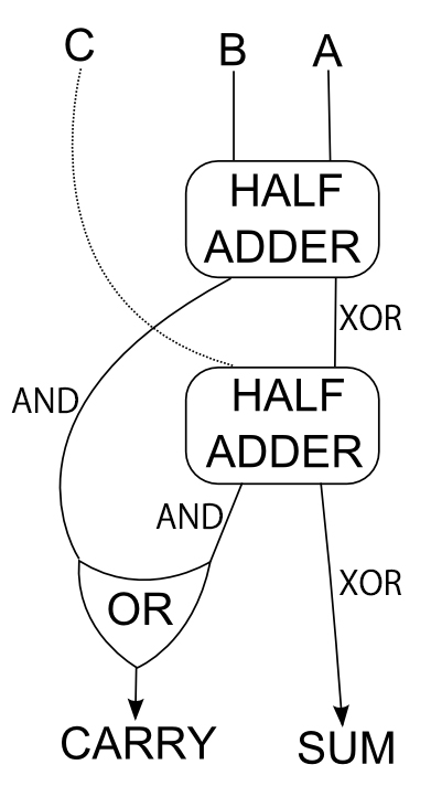
When you start thinking about a Full Adder it becomes obvious about how the Half Adder got its name.  The Full Adder is really just 2 half adders put together, plus a little extra bit to deal with the CARRY.  I made sure to map this out before trying to piece together the schematic:

full adder logic diagram

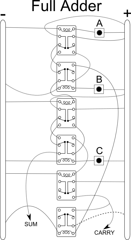
The OR gate in the bottom left is enough to handle the CARRY onto the next full adder.  If you start with a HALF ADDER and string together three Full Adders after it, then you have a 4-bit adder!  The rest of the work to designing the full adder was just the tedious matter of connecting all the dots:

relay Full adder

I encourage you to try and examine the diagram and follow the logic “flow” through the adder to see how it works.  The results of this circuit should be the same as a the results of the last three columns in the Excel adder.

Having designed the structures necessary to build a 4-bit adder, I really wanted to build the real deal.  Which is exactly what I did next.

Creating Relay Logic Gates

I am not a computer scientist.  Nor have I really had any CS courses.  Far from it.  I hold two degrees in literature and literary theory.  So, when I started to wonder how computers work (since I use them every day!) I had to go about teaching myself.  While I have some experience with contemporary programming languages, I also wanted to start with the building blocks of the computer age:

Logic gates. 

The beginnings of computing and logic gates starts with telephone companies in the early-mid 20th century, and telephone companies did this with relays.

So that is where I needed to start: create relay logic gates of my design.

DPDT Relays

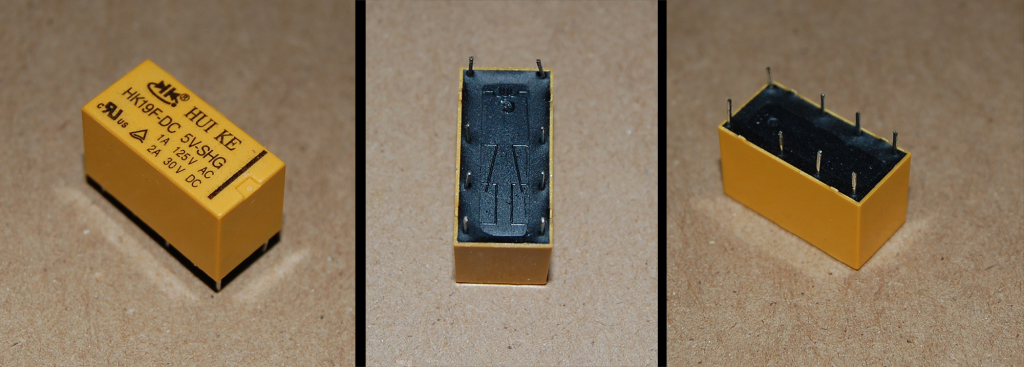
DPDT relay photo

 The first thing I did was order some relays.  Well, really the first thing I did was learn what relays are, what kinds there are, and what it is exactly that they do.  Then I went bargain hunting.  On Amazon I found some cheap 5 volt relays.  I wanted 5v because it was a voltage that I understood (USB runs off it, 4 AA batteries produce it).  These cheap relays were DPDT (double pole double throw) so I started drawing up some custom schematics for making some basic logic gates. 

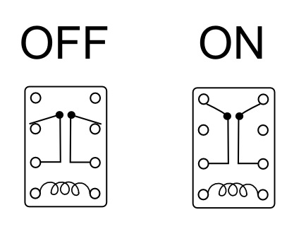
Firstly, I had to understand how a DPDT relay looks in its OFF state and its ON state in order to understand how to develop logic gates.

DPDT relay on off

 Relays work by having a mechanical switch that is triggered magnetically when a coil is electrified.  For my particular relays, putting 5V through the coil throws two switches from on OFF pole to an ON pole.  In the diagram above I repsesented the “hinge” of the switch as a little black dot.  Hopefully you can see how this works.  Essentially, in data terms, this gives you two binary bits controlled by a single input.  Both bits are zero (OFF) until the coil is powered, making them both 1 (ON).  Off course you don’t have to use both bits on a DPDT when building logic gates, but it can be useful.  A single pole double throw relay (SPDT) works the same way except it only controls a single bit.  A SPDT would work fine for building logic, it would just take more of them, and oddly enough DPDT switches seemed cheaper and easier to find.

With the relay as the basic building block, I set about designing my own logic gates.  The two basic logic gates are the AND gate and the OR gate.  I pulled this chart from the Wikipedia page on Logic Gates:

Type Boolean Truth Table
AND A & B
INPUT OUTPUT
A B A AND B
0 0 0
0 1 0
1 0 0
1 1 1
OR A or B
INPUT OUTPUT
A B A OR B
0 0 0
0 1 1
1 0 1
1 1 1

Relay AND Gate

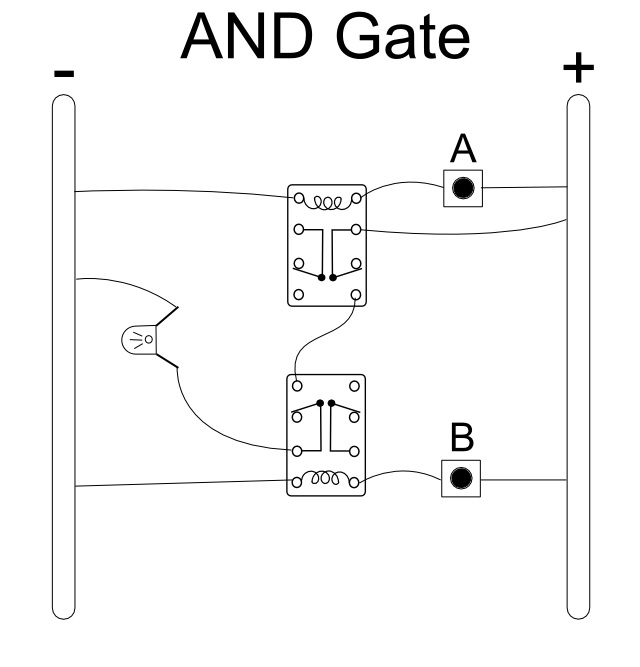
Truth tables are an important part of understanding basic computer logic, and they give me the clearest picture of what’s happening.  For example, look at the AND gate truth table above.  Only when input A and input B are 1 (meaning that they have a current flowing through them) does the output result in 1 (meaning that the electricity flows out of the gate.)  Using the truth table as a guide I desgined the following logic gate using my DPDT relays.

 relay AND gate

 The schematic setup looks a little like a breadboard because that is the easiest way for me to wrap my head around the design.  The right rail is positively charged while the left rail is connected to ground, giving it a negative charge.  A and B inputs here are represented by push-button switches that only allow a current through when pressed.  This just helped me to imagine turning A and B off and on as I was designing the circuit.

The object to the left of the relays is an LED so that I could conceptualize some kind of output.  If this were to be made into a real circuit the LED (depending on its type) would likely need a resistor behind it so that it doesn’t burn out at straight 5V.

While designing the circuits I tried to imagine following the flow of current down the lines from the positive rail as it passed through the buttons, relays, and LED all the way to the ground rail.  If the coil is activated as power passes through it then I conceptualized the relay switches being thrown and then tried to see if power could then flow through the relay in its on state.

Of course with the AND gate, the objective is to create a circuit where the LED is only supplied with power when both A & B input buttons are pressed.  The above schematic fulfills this objective.  No doubt there is a simpler way to do this, but I must remind you: I am am not a trained computer scientist.  That being said, what I did works for me.

Relay OR Gate

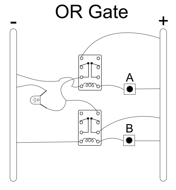
Making an OR gate can be relatively simple.  Some people would argue for simply wiring the output of the two buttons together directly to the LED.  However, this can lead to the current flowing backwards through your circuit and can cause problems as you develop more sophisticated logic from these building blocks.  So I made a simple OR gate using two DPDT relays:

relay OR gate

Looking at the Truth table above and the OR gate circuit, hopefully you can see how this results in a working OR gate.

With these basic logic gates sorted out, I could now think about doing something a little more advanced.  Using these basic logic gates (and one more type) I designed my own Half Adder and Full Adder circuits using relays.